


FPGA Device Migration.
Microcontroller programming with FPGA interfacing.
Data Converters and other peripheral board designs.
HDL code design for digital systems.
Open the Door to Your Imagination
Capabilities
Schematic Design Solutions
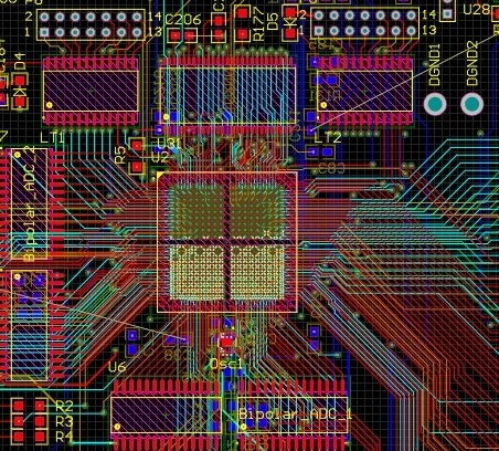
The very starting point in electronic system design is Schematic. Schematic Design is an initial and important part of the rest of the design and development process.
Mistakes in your schematic design can easily make their way all the way into prototypes or production without a second thought once the layout starts. Before the layout of schematics, design reviews are performed for their approval and often these tasks are time-consuming.
Many times these schematic reviews still let many issues pass through which are not found until the prototype is tested, as all too many companies are too pressed for time to come up with a formal design review checklist relevant to their products.
The logical design partitioning, components annotation, alignment, polarities, connectivity between components, placement of components, electrical rule checks and net directives are important aspects that must be considered before transferring the design onto a PCB.
Schematic design is also helpful in finding out circuit behavior by simulation and then changing components type and model accordingly. We, at RapidConnect Technologies, provide you with complete Schematic Design Services which will help you in reducing the design errors and iterations.

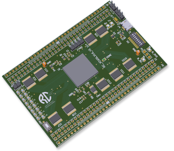
PCB Design
Transferring your schematic circuit into a PCB is important for the successful functioning of the electrical circuit. But there are points that need to be considered before transferring the design such as :
1. Whether your schematic is able to transfer into the PCB layout.
2. Do all the footprints of all the components as per the requirements or availability.
3. Do all the nets connected and defined or labeled properly.
4. Have you defined the partitioning of your design like high voltage, power, communication, low speed, and high-speed sections.
5. Do all the track widths for the different nets properly chosen.
6. Is your grounding clear in your design.
7. The layer stack should be done prior to fabrication and in consultation with fabrication.
8. Are you following the standards.
All these points must be answered before laying out a circuit in the form of PCB. Fortunately, RapidConnect Technologies can answer these points as per your requirements and provide you circuit layout for your schematic design.
Reflow Soldering
Once your PCB is fabricated, a bare PCB is of no use till it has components mounted. Components mounting is done through a soldering process which in principle is a simple process. Depending upon component package type, which can be through-hole, SMD, QFN or BGA, the process can be either by manual or through automated reflow process.
The fine pitch, QFN or BGA ICs are prone to damage when they exceed their temperature limit or do not follow the manufacturer specifications. The soldering method becomes important for reliability of circuit boards and ICs also.
We, at RapidConnect Technologies, follow the standard soldering process through our German Reflow system which not only follows standard temperature profiles as provided by the manufacturer but also safeguard ICs and boards from high temperatures.

Product development as per customization
Whether you are in the prototype stage or need replacement of costly boards with cost effective customized solutions, RapidConnect Technologies can help you develop your idea with more and better customization.